Surface Characterization
This system has the capability to:
- Perform Scanning Tunneling Microscopy measurements including tip preparation.
- Perform Atomic Force Microscopy Measurements including contact mode imaging, non-contact and tapping modes, and force modulation imaging.
Projects in Progress:
- AFM upgrades for force modulation system
Organic Spin-coating
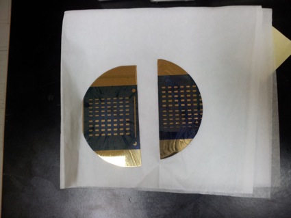
Organic thin film coating division consists of a spin coating system used for solution processing of organic materials. This facility is used to make thin films using a variety of substrates and solvents at room temperature. This system is fully operational and samples produced with the equipment have been measured with X-ray spectroscopy at the Canadian Light Source and Advanced Light Source at Berkeley labs, CA, as well as imaged with the AFM system described above. Currently under study are a set of molecules which are highly soluble and show desirable device characteristics such as high charge carrier mobility when they are prepared as spin-coated thin films.
Projects in Progress:
- Spin coating of materials for photovoltaics
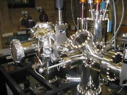
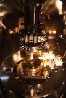
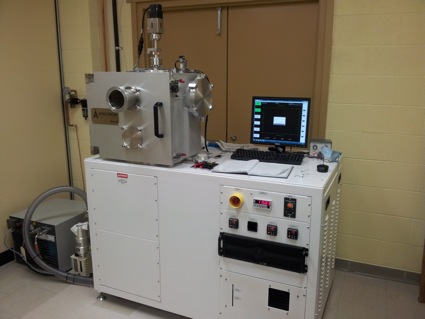
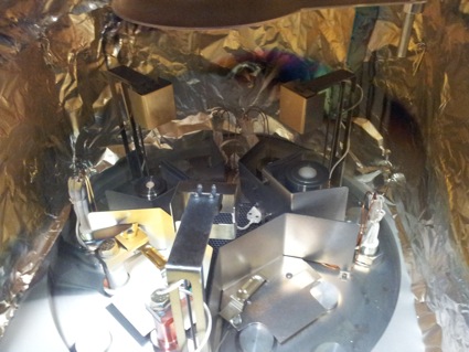
Thin Film Fabrication
This system has the capability to:
- Deposit thin films of metals and organic materials by vapor deposition.
- Measure I-V and C-V characteristics of thin film transistor devices
- Measure I-V characteristics of photovoltaic devices.
Projects in Progress:
- Sample Preparation for Spectroscopy Measurements
- Construction of Devices
Device Characterization
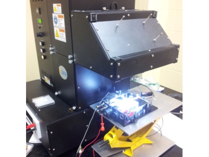
Solar Simulator and MOKE
The Device Characterization Division consists of a solar simulator and I-V measurement probe station, recently a Magneto-optic Kerr effect (MOKE) measurement system. The solar simulator is used for determining the power conversion efficiency of photovoltaic devices in conjunction with the probe station which is also equipped to measure the I-V curve of transistor devices. The MOKE is used to investigate the magnetization of materials.